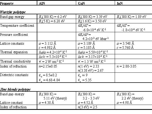
The best understood III-Nitride semiconductor is GaN, mainly because its bandgap of 3.39 eV makes it the best candidate for devices operating in the blue or UV part of the electromagnetic spectrum and it is the easiest to grow. In terms of lattice constants GaN is located between AlN on the low and InN on the high end as predicted by the periodic table and shown in Table 1, which gives an overview of the physical and electrical properties of the III-Nitride semiconductors. GaN has a high chemical stability at elevated temperatures (up to about 900ºC) and is suitable for caustic environments, but also presents a technological challenge in device manufacturing due to its high stability.
AlN is the smallest III-V nitride in terms of lattice constants. It is a very hard material, with high thermal conductivity, resistant to high temperatures and caustic chemicals. Those properties make it an ideal candidate for electronic packaging applications (Ref. 8).
InN is the least studied III-V nitride semiconductor. The main reason is that it is very hard to grow due to its low vapor pressure and instability above about 500°C (Ref. 1,8). It is also considered as having not to many applications due to the fact that it is active in a part of the electromagnetic spectrum that is already covered by well established conventional semiconductor technology (E_g = 1.89 eV). InN has uses in alloy systems though, so it is not just of interest purely for basic research.
The III-V semiconductors discussed can be alloyed in all mole fractions. Several systems are of particular interest. AlGaN has the potential to be used for devices active well into the UV part of the electromagnetic spectrum due to a bandgap larger than GaN.
GaN has a direct bandgap of 3.39 eV at room temperature. Therefore, as previously mentioned, it is well suited for devices operating in the blue to UV spectrum if the material is of high enough quality. Unintentionally doped GaN is the foremost problem in growing device quality material. Most material grown so far had been n-type of values typically in the range from 10^19 to 10^16 cm^-3. Since no impurities have so far been observed to account for such a large background carrier concentrations it is thought to be due to nitrogen vacancies. This became even more likely once p-type doping became possible and experimental results accompanying the doping effort suggest that N-vacancies are responsible for the large background carrier concentrations.
Since so far no way has been found to get totally rid of the n-type background carrier concentration most groups tried to compensate with shallow p-type dopants. Most potential dopants tried produced highly resistive material, but none seemed to generate p-type material. Doping GaN p-type was finally accomplished by Amano et. al. (Ref. 4) using Mg to grow compensated GaN and converting it to p-type material with low energy electrons (LEEBI). Nakamura et. al. improved on those results and were the first to report on the doping mechanism. Their layers were grown by atmospheric pressure MOVPE using cyclopentadienyl magnesium as the dopant gas (Ref. 5) and the compensated GaN became dramatically p-type after LEEBI treatment (Ref. 6) as shown in Table 2. The same group shortly after found that Mg-compensated GaN could equally well be converted to p-type conductive material by thermal annealing at 700°C under N_2 ambient (Ref. 7). This procedure is considered to be a big improvement over electron irradiation due to the fact that the entire bulk film is treated and converted in contrast to only the surface region down to the penetration depth of the electrons.
The mechanism behind the conversion from compensated Mg-doped GaN to p-type conducting GaN became clear after a series of experiments (Ref. 9) involving alternately annealing Mg-compensated GaN under N_2 and NH_3. Using N_2 GaN becomes p-type conductive, under NH_3 resistive. It became clear that a Mg-H neutral complex was responsible for compensating n-type GaN. Ohba and Hatano (Ref. 10) found that H-atom incorporation increases linearly with Mg concentration using secondary ion mass spectroscopy (SIMS). H-atom concentration significantly decreased after thermal treatment in Ar, indicating a H-atom extraction effect of the thermal treatment. The H atoms are thought to come from NH_3 used as the N source.
Compensated GaN was observed to have a large midgap photoluminescence (PL) emission and a relatively weak blue signal. The midgap signal was eliminated in p-type GaN produced by annealing under N_2 and the intensity of the blue emission was maximized by using an anneal temperature of 700°C (Ref. 7). Ohba and Hatano (Ref. 10) looked at the near-band-edge PL peak at 355 nm as a function of Mg concentration before and after thermal treatment in Ar. They found that for as-grown GaN the intensity increases monotonically with Mg concentration, but after thermal anneal the intensity is high at low Mg concentrations decreasing monotonically with Mg concentration. They also confirmed a deep-level emission peak after thermal anneal. The substantial increase of the PL intensity after thermal treatment at low Mg concentrations is presumably due to increase of carrier concentration.
Moustakas and Molnar (Ref. 11) successfully grew p-type GaN using exited N_2 and a MBE system taking advantage of the absence of H in a high vacuum (HV) system.


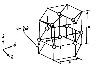
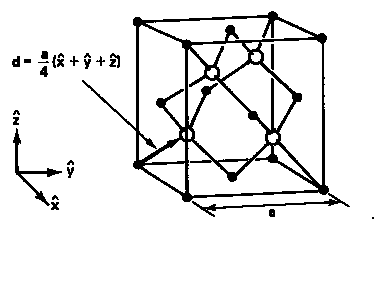
Figure 1: Wurtzite and Zinc Blende Crystal Structure

Table 1: Properties of III-Nitrides (Ref. 8)

Table 2: p-type GaN by LEEBI treatment (Ref. 6)
Table of Contents