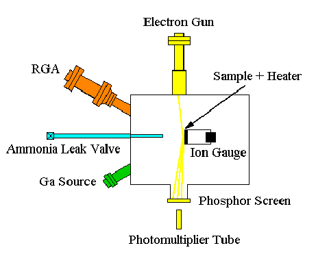
System
UNIVERSITY OF MINNESOTA
Department of Electrical Engineering
*also Department of Materials Science
Grzegorz Nowak, Izabella Grzegory, and Sylwester Porowski
POLISH ACADEMY OF SCIENCES
High Pressure Research Center
- presented at the MRS fall meeting in December 1997
- also presented at the PCSI-25 in January 1998
- to be submitted to Journal of Crystal Growth
- please contact authors for preprints and referencing
AFOSR F49620-95-1-0431 and ONR N-00014970063
Abstract
GaN was grown on bulk GaN samples by molecular beam epitaxy and compared to growth of GaN on sapphire. This work examines both surface polarities without the complication of a heteroepitaxial buffer. Well ordered epitaxial growth could be obtained on the GaN(0001(bar)) surface under a wide range of growth parameters. Smooth morphologies on the GaN(0001) surface were obtained under conditions of excess Ga, near 850°C.
Growth under excess N and step flow conditions on miscut samples produced a well ordered step train. These surfaces exhibited a 1x1 diffraction pattern during growth. After growth and cooling to room temperature, in the presence of NH3, missing line defects were observed. The defects were similar to those identified by Packard and Dow in the absence of N after annealing. Further, the low temperature Ga rich reconstructions reported by Feenstra and coworkers were observed only in the absence of NH3. By contrast, the GaN(0001) surface showed a weak 2x2 reconstruction at growth temperatures with excess Ga. The behavior of the RHEED intensity on both sides is shown to be different, which can be used to identify polarity and to set growth conditions.
Growth on the GaN(0001(bar)) surface was compared to growth on sapphire under a wide range of conditions. Under comparable conditions a lower hillock density and no pinholes were observed. Two main growth limits were examined for low-index surfaces. First, under conditions of excess Ga, growth was generally smoother on both bulk and sapphire substrates than under N rich conditions. Hillocks with meandering step edges and a mixture of c/2 and c height steps were observed. Second, under conditions of excess N, the bulk samples did not exhibit a strong tendency to 3D growth, unlike growth on sapphire. At lower NH3 fluxes RHEED intensity oscillations corresponded closely to growth of c/2 height monolayers of GaN. As the NH3 flux was increased, the period of growth increased. The period also increased with substrate temperature, with an activation energy that we identify with a surface diffusion process of 1.1 eV.
* This work was partially supported by the Office of Naval Research and by the Air Force Office of Scientific Research.
System

Polarity determination based on CBED by Liliental8 et al and Smith7 et al, contradicting results by Ponce10 et al.

The RHEED intensity behavior of the specular <2110> beam was recorded as a function of time on both GaN{0001} polarities, at typical growth temperatures of 800oC. Two stable surface terminations were observed on the GaN(0001(bar)) polarity, which can be obtained by exposing the surface to either Ga or NH3 only. The GaN(0001) polarity exhibits one stable surface termination only, and a reconstruction transition is observed depending on Ga coverage, which depends on Ga flux. We believe that this transition corresponds to the transition reported by Hacke9 et al. This difference in behavior can be used to identify polarity.

Low temperature surface reconstructions first observed by Smith7 et al are shown in this figure (c(6x12) not shown). We found that it is crucial to expose the GaN(0001) surface with Ga in the absence of NH3 first in order to obtain these reconstructions by adding additional Ga at low temperatures. The procedure of creating this stable Ga terminated GaN(0001) surface was described in the previous figure.

RHEED intensity oscillations were recorded using the specular <2110> beam. These oscillations were observed only under excess NH3 (Ga-limited) conditions, indicating growth by island nucleation. After closing the Ga shutter the RHEED intensity recovers above approx. 700oC. Continued growth at low temperatures eventually leads to a rough surface, but the samples can be annealed to their initial RHEED intensity.
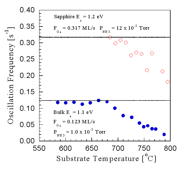
RHEED intensity oscillations were measured as a function of temperature on both bulk GaN and GaN on sapphire. We found that the oscillation frequency decreases with increasing temperature. No Ga was found to desorb from the surface using desorption mass spectroscopy (DMS).3,5 We attribute the reduction in oscillation frequency to a Ga diffusion process with an activation energy of 1.1 eV, resulting in a transition from island nucleation to step flow growth.
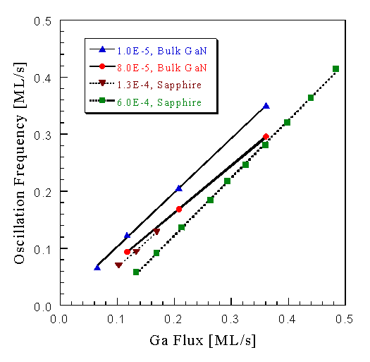
This figure shows the RHEED intensity oscillation frequency as a function of Ga flux at different NH3 fluxes. The substrate temperature was kept at approx. 650oC, and data for both bulk GaN and GaN on sapphire are shown. The oscillation frequency increases linearly for all NH3 fluxes, but the slope is not unity ranging from 0.8 to 1.0. An offset is observed as well. No satisfying explanation has been found yet to explain this behavior.
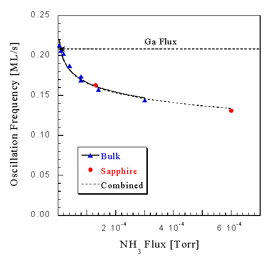
In an effort to explain the data obtained in the previous figure we investigated the dependence of the RHEED intensity oscillations on NH3 flux. This figure shows the oscillation frequency as a function of NH3 flux, at a fixed temperature of approximately 650oC. The frequency reduction is least pronounced close to NH3-limited (excess Ga) growth, and levels off with increasing NH3 flux. Data taken from GaN on sapphire fit the bulk data well. Even with this additional data we are still unable to explain this behavior by a simple model.
GaN(0001(bar)) on bulk GaN and GaN(0001(bar)) on Sapphire
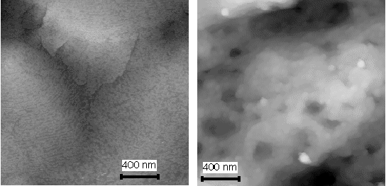
Under excess Ga conditions, surfaces of GaN grown on bulk GaN(0001(bar)) were smoother than surfaces of GaN grown on sapphire{0001}. The bulk GaN(0001(bar)) surface had a lower hillock density and no pinholes. Typically, GaN grown on sapphire contains pinholes that are believed to originate at the GaN/sapphire interface. The smoother bulk GaN(0001(bar)) surface demonstrates potential benefits of homoepitaxial growth in the fabrication of electronic devices. For example, smoother surfaces enable smoother interfaces and better electrical contacts.
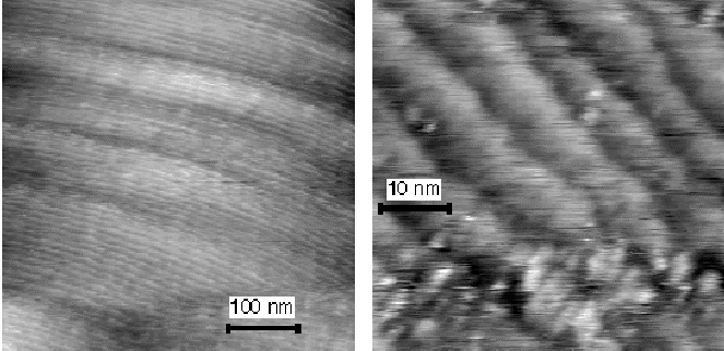
Under excess N and step flow conditions, GaN growth on a GaN(0001(bar)) substrate polished 2 degrees toward the <0110> produced a well ordered step train. The step heights were c/2 where c is the height of a conventional cell. After growth and cooling to room temperature in an ammonia flux, missing line defects were observed that were perpendicular to the step edges. The separation between line defects was 2.5 nm. This structure is similar to that identified by Packard and Dow6, who heated GaN on sapphire to high temperature in the absence of any fluxes.
Growth under Excess Ga and Excess N Conditions
Surfaces of GaN on low index GaN(0001(bar)) substrates were smoothest when grown under excess Ga conditions. This was indicated by smaller and fewer hillocks on the GaN surface. As explained in the next figure, the hillocks produced under excess Ga conditions are characteristically different from hillocks produced under excess N conditions.

Depending on growth conditions, two types of hillocks with different characteristics were observed on surfaces of GaN grown on bulk GaN(0001(bar)). Under excess Ga conditions, hillocks were shorter with rounded bases and few macrosteps; in addition, STM showed meandering steps with a mixture of c/2 and c heights. Under excess N conditions, hillocks were taller with hexagonal, faceted bases.

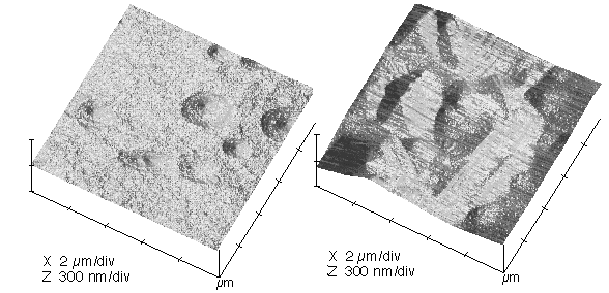
This panel contains AFM images from a GaN(0001) surface after 120 min of growth at approx. 800oC, with a Ga flux of 1.3 ML/s and an NH3 BEP of 1x10⁻⁵ Torr. The large scale image shows groves left from the mechanical polishing process. Zooming in we see domains of different height with raised perimeters. These domains contain steps, some of which intersect at angles consistent with the hexagonal crystal symmetry.
2 "Chemical polishing of bulk and epitaxial GaN", J. Weyher, S. Muller, I. Grzegory, S. Porowski, Journal of Crystal Growth, to be published
3 "In Situ Control of GaN Growth by Molecular Beam Epitaxy", R. Held, D.E. Crawford, A.M. Johnston, A.M. Dabiran, and P.I. Cohen, Journal of Electronic Materials, 26, 272 (1997)
4 "Growth Rate Reduction of GaN Due to Ga Surface Accumulation", D.E. Crawford, R. Held, A.M. Johnston, A.M. Dabiran, and P.I. Cohen, MRS Internet Journal of Nitride Semiconductor Research, 1, 12 (1996)
5 "N-Limited versus Ga-Limited Growth of GaN (0001(bar)) by MBE using NH3", R. Held, D. E. Crawford, A. M. Johnston, A. M. Dabiran, and P. I. Cohen, Surface Review and Letters, accepted for publication as review
6 "Scanning tunneling microscopy of the GaN(0001) surface", W.E. Packard, J.D. Dow, R. Nicolaides, K. Doverspike, R. Kaplan, Superlattices & Microstructures, 20, 145 (1996)
7 "Reconstructions of the GaN(0001(bar)) Surface", A.R. Smith, R.M. Feenstra, D.W. Greve, J. Neugebauer, and J.E. Northrup, submitted to Physical Review Letters
8 "Structural Characterization of Bulk GaN Crystals Grown Under High Hydrostatic Pressure", Z. Liliental-Weber, C. Kisielowski, S. Ruvimov, Y. Chen, J. Washburn, I. Grzegory, M. Bockowski, J. Jun, and S. Porowski, Journal of Electronic Materials, 25, 1545 (1996)
9 "Monitoring surface stoichiometry with the (2x2) reconstruction during growth of hexagonal-phase GaN by molecular beam epitaxy", P. Hacke, G. Feuillet, H. Okumura, and S. Yoshida, Applied Physics Letters, 69, 2507 (1996)
10 "Determination of lattice polarity for growth of GaN bulk single crystals and epitaxial layers", F.A. Ponce, D.P. Bour, W.T. Young, M. Saunders, J.W. Steeds, Applied Physics Letters, 337, 69 (1996)
Back to my home page